Sequential logic circuits
A logical circuit whose outputs are a logical function of it's inputs and it's current state. Unlike combinatorial logic circuits, these circuits have some element of memory.
Flip flops
A flip flop is the most basic memory circuit. It has two stable states (bistable) which allows it to store a single bit of data. The state can be changed by activating some control input. The circuit below shows an $\overline{SR}$ NAND latch.
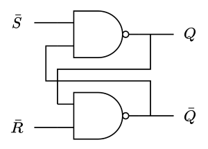
$\bar{S}$ and $\bar{R}$ are set and reset inputs respectively. The NAND latch is active low, hence the bars over the inputs. $Q$ and $\bar{Q}$ are the outputs and $\bar{Q}$ is the inverse of $Q$. Both inputs should never be active at the same time. The latch has the following truth table (remember it's active low):
| $S$ | $R$ | $Q$ | $\bar{Q}$ |
|---|---|---|---|
| 1 | 1 | No change | No change |
| 1 | 0 | 1 | 0 |
| 0 | 1 | 0 | 1 |
| 0 | 0 | Invalid | Invalid |
D-type latch
A D-type latch is created using the $\overline{SR}$ NAND latch. It has one data input and an enable line. The state will only be modified when the enable line is high. The design of the circuit prevents the invalid state because when the enable line is low both are high and if the enable line is high the negation ensures only one is ever low at a time. Note that the D-type latch is active high.
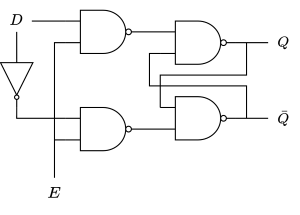
| $D$ | $E$ | $Q$ | $\bar{Q}$ |
|---|---|---|---|
| 0 | 0 | No change | No change |
| 1 | 0 | No change | No change |
| 0 | 1 | 0 | 1 |
| 1 | 1 | 1 | 0 |
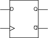
The enable line is often connected to a clock. The state of the D-type is then changed on the rising edge of the clock (from 0 to 1). The D-type latch is often represented as below, where the $>$ input is the enable line/clock input.
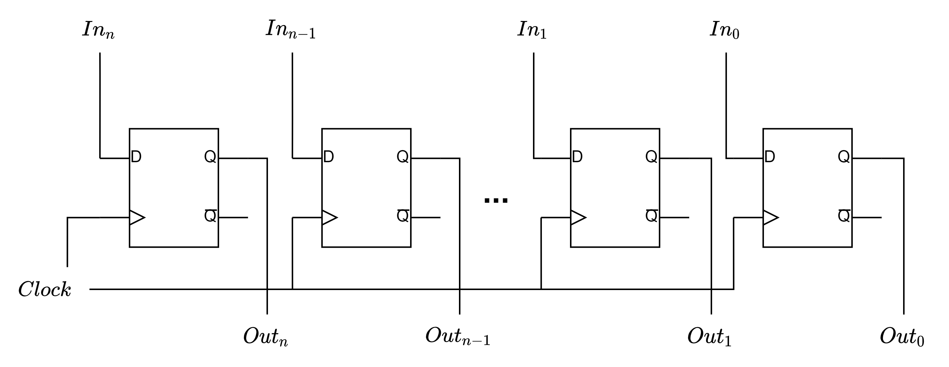
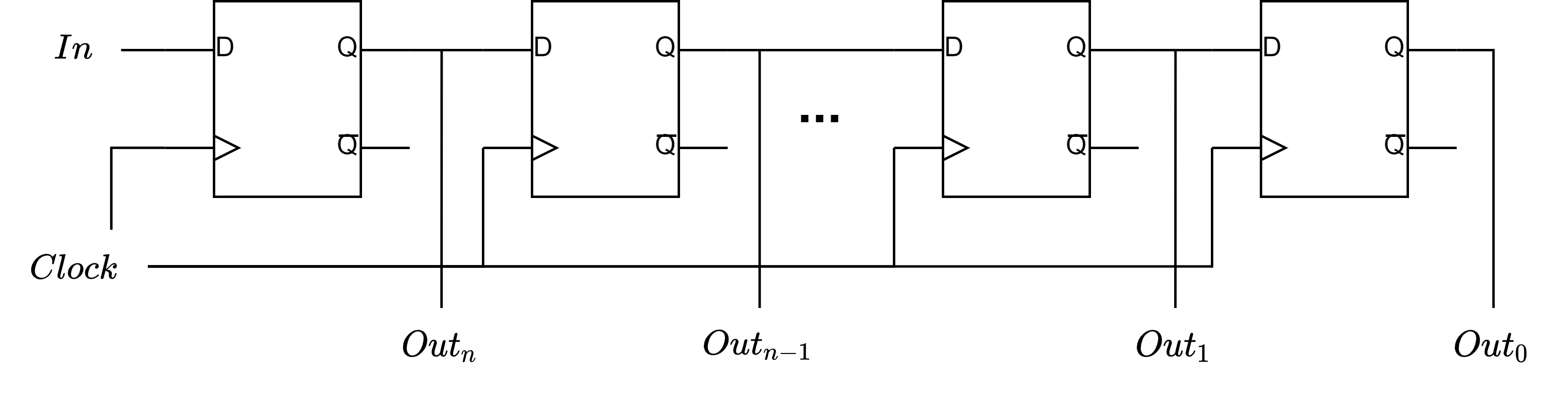
N-bit register
The n-bit register is made from multiple D-type latches. A register can have parallel or serial inputs and outputs. Parallel is all the bits at once, serial is one bit at a time. The register below is a parallel in/parallel out n-bit register.
N-bit shift register
A shift register shifts it's contents every clock tick. The below register is a serial in/parallel out n-bit shift register.
N-bit counter
The n-bit counter counts up in binary. The leftmost D-type is clocked as normal. Every D-type has it's input as it's inverted output. Each subsequent D-type is triggered on the falling edge of the previous D-type (represented by the circles on the clock input below).
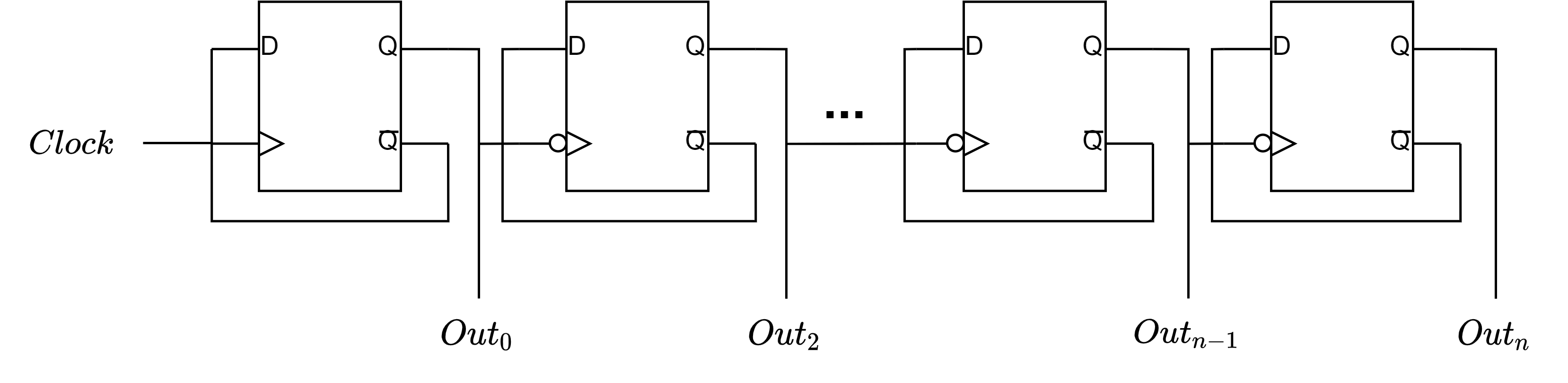
The n-bit counter works as follows:
Initial: The clock is low, the output of all D-types is 0.
Rising edge 1: The first D-type is clocked on the rising edge of the clock. $Out_0$ is now 1 because that was the value of $\bar{Q}$. The output has risen, so the second D-type is not clocked. Reading right to left, the output is now 00...0001, binary for 1.
Rising edge 2: The first D-type is clocked, it's input is $\bar{Q} = 0$, so the output is now 0. The output has fallen from 1 to 0, so the second D-type is now clocked. It's input is 1, so it's output is now 1. Reading right to left the output is now 00...0010, binary for 2.
Rising edge 3: The first D-type is clocked and is now 1. The output has risen so the second is not clocked. The overall output is now 00..0011, binary for 3.
Rising edge 4: The first D-type is clocked and is now 0. The output has fallen so the second D-type is clocked and is now 0. The second D-type output has fallen so the third D-type is clocked and is now 1. The overall output is now 00..0100, binary for 4.
This pattern will then repeat, counting up in binary.
Three state logic
Logic components considered so far have two states, 1 or 0. A 3-state buffer has an additional state, unconnected activated by the $\overline{Enable}$ line, which is active low.
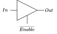
When $\overline{Enable}$ is high the buffer is unconnected, when it is low the input and output are connected. Three state buffers allow shared buses by allowing one data source on to the bus at once.
Physical implementations
Propagation delay
Propagation delay is the time taken for a logic gate to work, usually nanoseconds. This limits the speed at which logic circuits can work. Propagation delay can be reduced by making gates physically closer.
Integrated circuits
An integrated circuit is a collection of components on a single chip. These can be simple logic gates or programmable devices which allow larger circuits to be created. Programmable logic devices include the following:
-
Programmable Array Logic (PAL) - Programmable AND array and fixed OR array.
-
Programmable Logic Array (PLA) - Programmable AND and OR arrays.
-
Field Programmable Gate Array (FPGA) - Array of programmable logic blocks, which can be used for complex combinational functions or simple logic gates. FPGAs are usually reprogrammable.